
 |
21. Mirjalili, S., Ikbal, M. A., Hou, C.-W., Kalateh Mohammadi, M., Choi, Y., Kelbauskas, L., VanBlargan, L. A., Hogue, B. G., Murugan, V., Diamond, M. S., & Wang, C. (2025). Nanoparticle-supported, rapid, digital quantification of neutralizing antibodies against SARS-CoV-2 variants. Biosensors and Bioelectronics, 117549. https://doi.org/10.1016/j.bios.2025.117549.. |
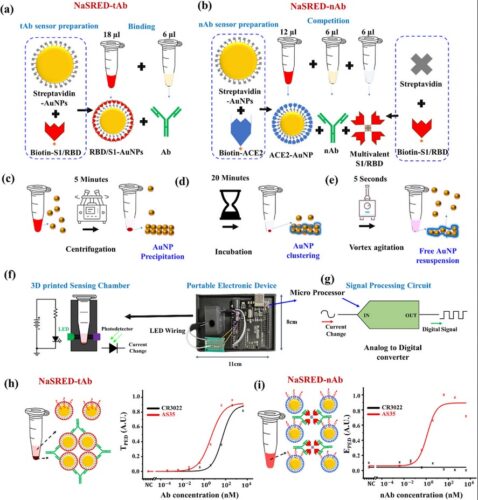
| Here, we report a rapid, low-cost, and portable assay for quantifying the neutralizing potency of antibodies against SARS-CoV-2 variants. Our platform, NasRED-nAb, leverages gold nanoparticles (AuNPs) functionalized with human ACE2 receptors to assess how effectively monoclonal antibodies and serum samples inhibit the spike (S) protein binding. The competitive binding event modulates AuNP aggregation and sedimentation, which is digitized using a semiconductor-based optical readout. The assay requires no labeling, washing, or enzymatic amplification, delivering results in less than 30 minutes with high sensitivity and specificity for different SARS-CoV-2 strains (Wuhan-Hu-1, Gamma, Omicron). Unlike conventional PRNT or ELISA-based methods, NasRED-nAb operates in a simple, single-tube, solution-phase format, making it suitable for near point-of-care applications. Its modular design, rapid turnaround, and low material cost position it as a valuable tool for evaluating vaccine efficacy, immune responses, and therapeutic antibody potency against emerging viral variants. |
 |
20. Mohammadi, M. K., Mirjalili, S., Ikbal, M. A., Xie, H., & Wang, C. (2025). Rapid and Sensitive Detection of Thrombospondin-2 Using Nanoparticle Sensors for Cancer Screening and Prognosis. Micromachines, 16(3), 354. https://doi.org/10.3390/mi16030354. |
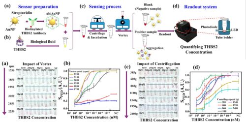
| In this study, we developed a rapid and sensitive assay platform for the detection of thrombospondin-2 (THBS2), a critical prognostic biomarker for various cancers including pancreatic, colorectal, and breast cancers. Leveraging the Nanoparticle-Supported Rapid Electronic Detection (NasRED) framework, gold nanoparticles (AuNPs) functionalized with THBS2-specific antibodies were used to capture target proteins from minimal sample volumes in a single-tube, in-solution assay. The assay integrates active fluidic forces, including centrifugation and vortexing, to enhance reaction kinetics and signal specificity, forming AuNP clusters upon THBS2 binding and enabling rapid colorimetric readout. Optical extinction signals were digitized using a portable semiconductor-based electronic device, providing a high sensitivity at femtomolar levels, a large dynamic range (five orders of magnitude), and high specificity against interfering biomarkers like CA19-9 and BSA. NasRED’s simple workflow, rapid turnaround (15 minutes), low material cost, and compatibility with complex fluids (serum, saliva, cerebrospinal, and synovial fluids) highlight its potential as an accessible and minimally invasive tool for early cancer screening and prognosis at point-of-care settings |
 |
19. Jiawei Zuo, Ashutosh Bangalore Aravinda Babu, Mo Tian, Jing Bai, Shinhyuk Choi, Hossain Mansur Resalat Faruque, Smitha S. Swain, Michael N. Kozicki, Chao Wang, and Yu Yao*, “Metasurface-Based Muller Matrix Microscope,” Advanced Functional Materials, pp. 2405412, DOI: 10.1002/adfm.202405412, 2024. |
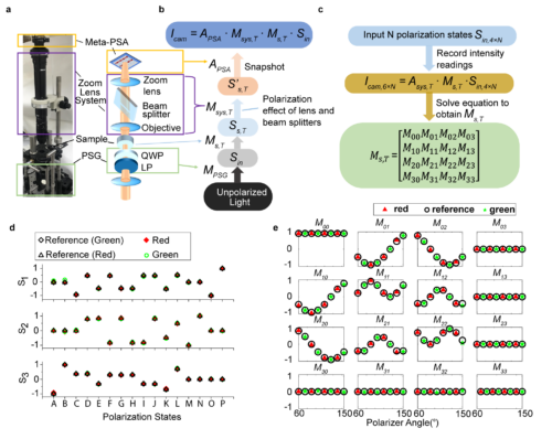
| Here, the study demonstrates a metasurface-based Muller matrix optical microscopes (MMM), i.e., Meta-MMM, which is equipped with a chip-integrated, single-shot metasurface polarization state analyzer (Meta-PSA). The Meta-MMM is featured with high-speed measurement (≈2s per Muller matrix (MM) image), superior operation stability, dual-color operation, and high measurement accuracy (measurement error 1–2%) for MM imaging. The Meta-MMM is applied to nanostructure characterization, surface morphology analysis, and discovering birefringent structures in honeybee wings. The Meta-MMMs hold the promise to revolutionize various applications from biological imaging, medical diagnosis, and material characterization to industry inspection and space exploration. |
 |
18. Shinhyuk Choi†, Jiawei Zuo†, Nabasindhu Das, Yu Yao*, and Chao Wang*, “Scalable Nanoimprint Manufacturing of Multi-Layer Hybrid Metasurface Device,” Advanced Functional Materials, pp. 2404852, DOI: 10.1002/adfm.202404852, 2024. |
| Optical metasurfaces, consisting of subwavelength-scale meta-atom arrays, hold great promise to overcome fundamental limitations of conventional optics. Scalable nanomanufacturing of metasurfaces with high uniformity and reproducibility is key to technology transfer and commercialization. Recently, nanoimprint lithography (NIL) has attracted increasing interests for metasurface fabrication because of its superior nanometer resolution, rapid prototyping and large-area manufacturing capabilities. Despite NIL demonstrations of single-layer metasurface, scalable fabrication of double- and multi-layer metasurfaces remains challenging. Here we leverage the high resolution and 3D pattern transfer capabilities of NIL to collaboratively design and fabricate multi-layered metasurfaces for on-chip polarimetric imaging devices. Our process achieved sub-100 nm nanostructures, sub-200 nm alignment accuracy, and nanometer-scale linewidth uniformity over >20 mm2. This NIL-based, low-cost and high-throughput nanomanufacturing approach paves the way toward scalable production of a plethora of metasurface structures for ultra-compact optic and optoelectronic devices and systems. |
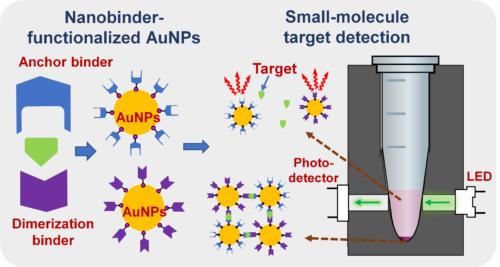 |
17. MD Ashif Ikbal†, Shoukai Kang†, Xiahui Chen, Liangcai Gu*, and Chao Wang*, , “Picomolar-Level Sensing of Cannabidiol by Metal Nanoparticles Functionalized with Chemically Induced Dimerization Binders,” ACS Sensors, vol. 8, pp. 4696–4706, 2023. https://doi.org/10.1021/acssensors.3c01758. |
| Here, we developed a generalizable method for highly sensitive and specific in-solution detection of small molecules, using cannabidiol (CBD) as an example. Our sensing platform uses gold nanoparticles (AuNPs) functionalized with a pair of chemically induced dimerization (CID) nanobody binders (nano-binders), where CID triggers AuNPs aggregation and sedimentation in the presence of CBD. Despite moderate binding affinities of the two nano-binders to CBD (equilibrium dissociation constants KD of ~6 and ~56 µM), a scheme consisting of CBD-AuNP pre-analytical incubation, centrifugation, and electronic detection (ICED) was devised to demonstrate a high sensitivity (limit of detection of ~100 picomolar) in urine and saliva, a relatively short sensing time (~2 hours), a large dynamic range (5 logs), and a sufficiently high specificity to differentiate CBD from its analog, tetrahydrocannabinol. The high sensing performance was achieved with the multivalency of AuNP sensing, the ICED scheme that increases analyte concentrations in a small assay volume, and a portable electronic detector. This sensing system is readily applicable for wide molecular diagnostic applications. |
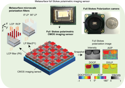 |
16. Jiawei Zuo, Jing Bai, Shinhyuk Choi, Ali Basiri, Xiahui Chen, Chao Wang, and Yu Yao*, “Chip-Integrated Full-Stokes Polarimetric CMOS Imaging Sensor,” Light: Science & Applications, vol. 12, pp. 218, 2023. https://doi.org/10.1038/s41377-023-01260-w. |
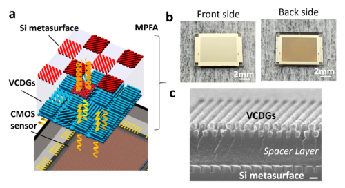
| Polarimetric imaging has a wide range of applications for uncovering features invisible to human eyes and conventional imaging sensors. Here we present a chip-integrated Metasurface-based Full-Stokes Polarimetric Imaging sensor (MetaPolarIm) realized by integrating an ultrathin (~600 nm) metasurface polarization filter array (MPFA) onto a visible imaging sensor with CMOS compatible fabrication processes. The MPFA is featured with broadband dielectric-metal hybrid chiral metasurfaces and double-layer nanograting polarizers. This chip-integrated polarimetric imaging sensor enables single-shot full-Stokes imaging (speed limited by the CMOS imager) with the most compact form factor, record high measurement accuracy, dual-color operation (green and red) and a field of view up to 40 degrees. MetaPolarIm holds great promise to enable transformative applications in autonomous vision, industry inspection, space exploration, medical imaging and diagnosis. |
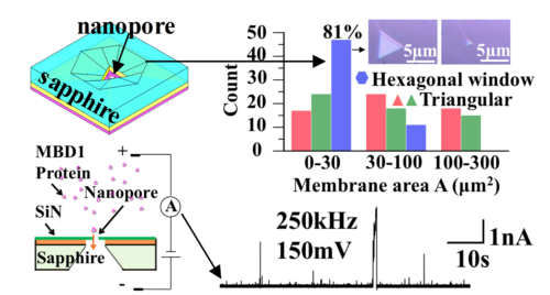 |
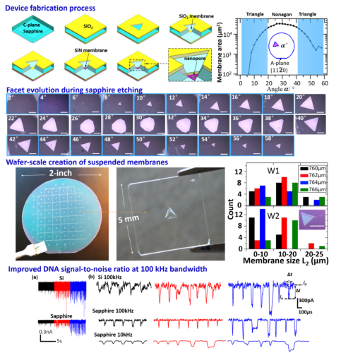
15. Pengkun Xia, Md Ashiqur Rahman Laskar, and Chao Wang, “Wafer-Scale Fabrication of Uniform, Micrometer-Sized, Triangular Membranes on Sapphire for High-Speed Protein Sensing in a Nanopore,” ACS Applied Materials & Interfaces, vol. 15, pp. 2656–2664, 2023. |
| Ultra-low-noise solid-state nanopores are attractive for high-accuracy single-molecule sensing. A conventional silicon platform introduces acute capacitive noise to the system, which seriously limits the recording bandwidth. Recently, we have demonstrated the creation of thin triangular membranes on an insulating crystal sapphire wafer to eliminate the parasitic device capacitance. Uniquely different from the previous triangular etching window designs, here hexagonal windows were explored to produce triangular membranes by aligning to the sapphire crystal within a large tolerance of alignment angles (10–35°). Interestingly, sapphire facet competition serves to suppress the formation of more complex polygons but creates stable triangular membranes with their area insensitive to the facet alignment. Accordingly, a new strategy was successfully established on a 2 in. sapphire wafer to produce chips with an average membrane side length of 4.7 μm, an area of <30 μm2 for 81% chips, or estimated calculated membrane capacitance as low as 0.06 pF. We finally demonstrated <4 μs high-speed and high-fidelity low-noise protein detection under 250 kHz high bandwidth. |
 |
14. Shinhyuk Choi †, Zhi Zhao, Jiawei Zuo, Hossain Mansur Resalat Faruque, Yu Yao, and Chao Wang*, “Structural color printing via polymer-assisted photochemical deposition,” Light: Science & Application, vol. 11, pp. 84, 2022. https://doi.org/10.1038/s41377-022-00776-x |
| Structural color printings have broad applications due to their advantages of long-term sustainability, eco-friendly manufacturing, and ultra-high resolution. However, most of them require costly and time-consuming fabrication processes from nanolithography to vacuum deposition and etching. Here, we demonstrate a new color printing technology, a room temperature, ambient, and additive manufacturing process without requiring heating, vacuum deposition or etching. The capability of 3D metal printing both ultra-thin (~5 nm) composite films and highly reflective thicker film greatly benefit the design and construction of multilayered Fabry–Perot (FP) cavity structures to exhibit vivid and saturated colors. We demonstrated programmed printing of complex pictures of different color schemes at a high spatial resolution of ~6.5 μm. Finally, PPD-based color picture printing is demonstrated on a wide range of substrates, including glass, PDMS, and plastics. |
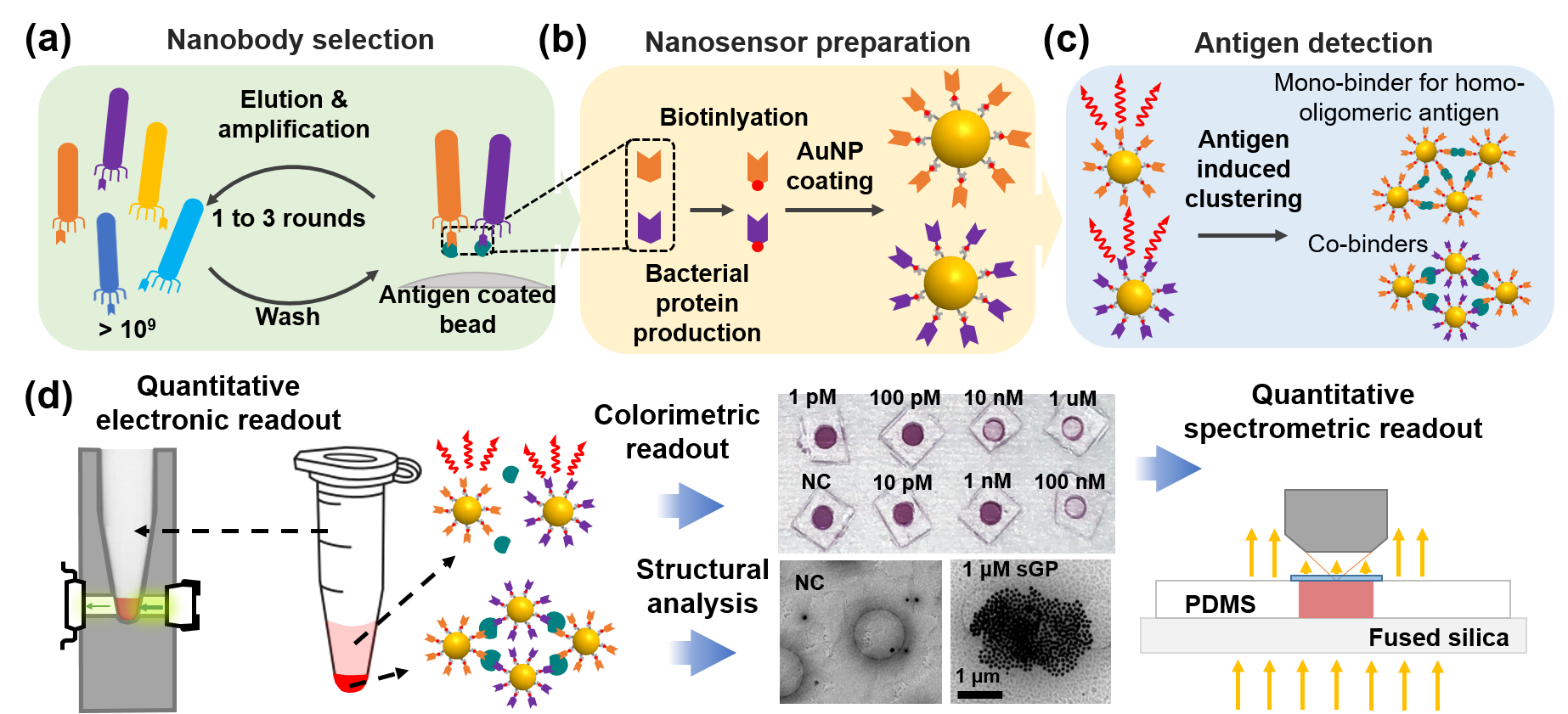 |
13. Xiahui Chen, Shoukai Kang, MD Ashif Ikbal, Zhi Zhao, Yuxin Pan, Jiawei Zuo, Liangcai Gu*, and Chao Wang*, “Rapid Electronic Diagnostics of Ebola Virus with Synthetic Nanobody-Conjugated Gold Nanoparticles,” Biosensors & Bioelectronics, vol. 202, pp. 113971, 2022. doi.org/10.1016/j.bios.2022.113971, also available at bioRxiv 2021.05.09.443341. (Biorxiv link; Biosensors & Bioelectronics link) |
| Successful control of emerging infectious diseases requires accelerated development of fast, affordable, and accessible assays to be widely implemented at a high frequency. Here we present a generalizable assay platform, nanobody-functionalized nanoparticles for rapid, electronic detection (Nano2RED), demonstrated in the detection of Ebola and COVID-19 antigens. To efficiently generate high-quality affinity reagents, synthetic nanobody co-binders and mono-binders with high affinity, specificity, and stability were selected by phage display screening of a vastly diverse, rationally randomized combinatorial library, bacterially expressed and site-specifically conjugated to gold nanoparticles (AuNPs) as multivalent in-solution sensors. Without requiring fluorescent labelling, washing, or enzymatic amplification, these AuNPs reliably transduce antigen binding signals upon mixing into physical AuNP aggregation and sedimentation processes, displaying antigen-dependent optical extinction readily detectable by spectrometry or simple electronic circuitry. With nanobodies against an Ebola virus secreted glycoprotein (sGP) and a SARS-CoV-2 spike protein receptor binding domain (RBD) as targets, Nano2RED showed a high sensitivity (limit of detection of ∼10 pg/mL for sGP and ∼40 pg/mL for RBD in diluted human serum), a high specificity, and a large dynamic range (∼7 logs). Unlike conventional assays where slow mass transport for surface binding limits the assay time, Nano2RED features fast antigen diffusion at micrometer scale, and can be accelerated to deliver results within a few minutes. The rapid detection, low material cost (estimated < $0.01 per test), inexpensive and portable readout system (< $5 and < 100 cm3), and digital data output, make Nano2RED particularly suitable for screening of patient samples with simplified operation and accelerated data transmission. Our method is widely applicable for prototyping diagnostic assays for other antigens from new emerging viruses. |
 |
12. Zhi Zhao †, Xiahui Chen, Jiawei Zuo, Ali Basiri, Shinhyuk Choi, Yu Yao, Yan Liu *, and Chao Wang *, “Deterministic Assembly of Single Emitters in Sub-5 Nanometer Optical Cavity Formed by Gold Nanorod Dimers on Three-Dimensional DNA Origami ” Nano Research, 2021, https://doi.org/10.1007/s12274-021-3661-z. (arXiv:2104.02916 ; Springer Nature Content Sharing Initiative) |
| Controllable strong interactions between a nanocavity and a single emitter is important to manipulating optical emission in a nanophotonic systems but challenging to achieve. Here a three-dimensional DNA origami, named as DNA rack (DR) is proposed and demonstrated to deterministically and precisely assemble single emitters within ultra-small plasmonic nanocavities formed by closely coupled gold nanorods (AuNRs). The DR uniquely possesses a saddle shape with two tubular grooves that geometrically allows a snug fit and linearly align two AuNRs with a bending angle <10°. It also includes a spacer at the saddle point to maintain the gap between AuNRs as small as 2-3 nm, forming a nanocavity estimated to be 20 nm3 and an experimentally measured factor of 7.3. A DNA docking strand is designed at the spacer to position a single fluorescent emitter at nanometer accuracy within the cavity. Using Cy5 as a model emitter, a ~30-fold fluorescence enhancement and a significantly reduced emission lifetime (from 1.6 ns to 670 ps) were experimentally verified, confirming significant emitter-cavity interactions. |
 |
11. Pengkun Xia, Jiawei Zuo, Pravin Paudel, Shinhyuk Choi, Xiahui Chen, Md Ashiqur Rahman Laskar, Jing Bai, Weisi Song, JongOne Im, Chao Wang*, “Sapphire-Supported Nanopores for Low-Noise DNA Sensing,” Biosensors and Bioelectronics, doi.org/10.1016/j.bios.2020.112829, 2020. (Link: https://www.sciencedirect.com/science/article/abs/pii/S0956566320308150; Full access until Jan 2021: https://authors.elsevier.com/a/1cCuk3PVtpkT%7Es; Also available on BioRxiv, Link: https://www.biorxiv.org/content/10.1101/2020.03.02.973826v1) |
| Solid-state nanopores have broad applications in single-molecule biosensing and diagnostics, but their high electrical noise associated with a large device capacitance has seriously limited both their sensing accuracy and recording speed. Current strategies to mitigate the noise has focused on introducing insulating materials (such as polymer or glass) to decrease the device capacitance, but the complex process integration schemes diminish the potential to reproducibly create such nanopore devices. Here, we report a scalable and reliable approach to create nanopore membranes on sapphire with triangular shape and controlled dimensions by anisotropic wet etching a crystalline sapphire wafer, thus eliminating the noise-dominating stray capacitance that is intrinsic to conventional Si based devices. We demonstrate tunable control of the membrane dimension in a wide range from ~200 μm to as small as 5 μm, which corresponds to <1 pF membrane capacitance for a hypothetical 1-2 nm thick membrane. .. |
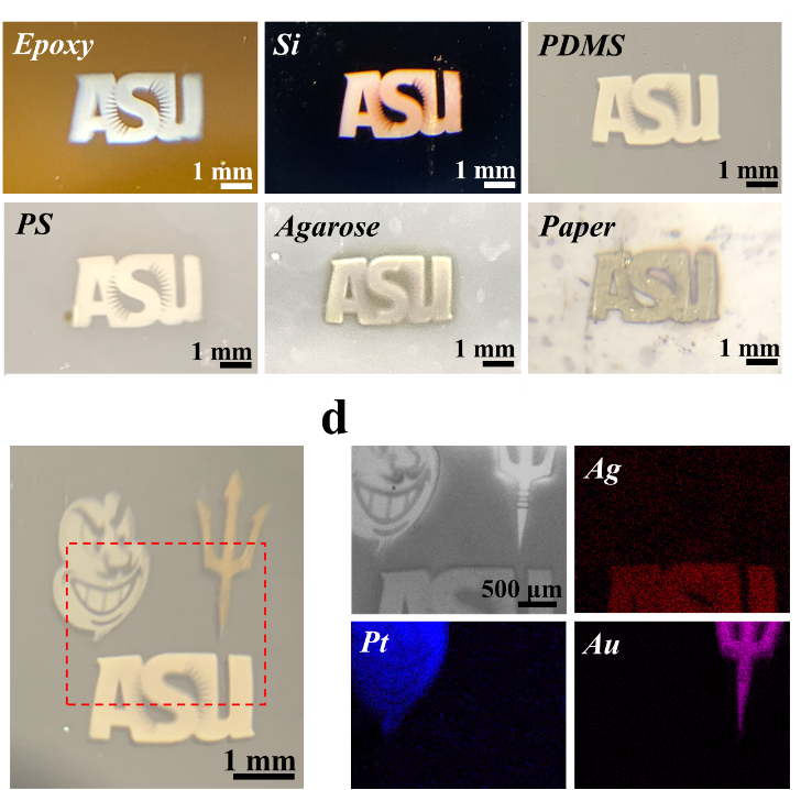 |
10. Zhi Zhao*, Jing Bai, Yu Yao, and Chao Wang*, “Printing Continuous Metal Structures via Polymer-Assisted Photochemical Deposition,” Materials Today, vol. 37, pp. 10-17, 2020. |
| Patterning complex metallic structures via additive manufacturing (AM) has broad applications in energy, medical and aerospace industries. Current AM methods are often limited by high processing temperature, discontinuous film deposition and/or low product conductivity and reflectivity. We present a versatile room-temperature metal printing technique based on polymer-assisted photochemical deposition (PPD). Two-dimensional (2D) and three-dimensional (3D) printing of silver, gold and platinum structures with feature sizes as small as 5 µm are demonstrated on various substrates, including silicon, glass, polymers and biocompatible hydrogels. The PPD-printed metal films are continuous and smooth (roughness <3 nm) even at ultra-low thicknesses (<10 nm), and highly conductive (~3105 S cm-1) and reflective comparable to that of vacuum deposited counterparts. This breakthrough in advanced AM technique holds great promise for low-cost, fast and distributed manufacturing in optics, electronics and robotics. |
 |
9. Zhi Zhao †, Chao Wang, Hao Yan *, and Yan Liu *, “Soft Robotics Programmed with Double Crosslinking DNA Hydrogels,” Advanced Functional Materials, pp. 1905911, 2019. (Link: https://onlinelibrary.wiley.com/doi/full/10.1002/adfm.201905911) |
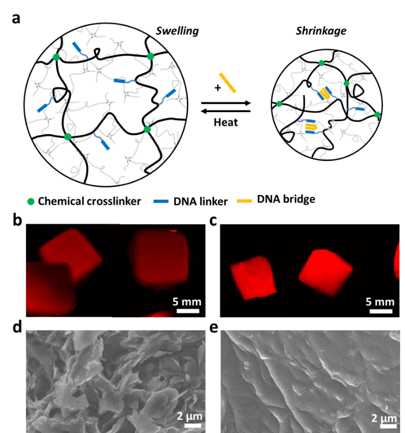
| Being the genetic material of living organisms, DNA molecules should have the intrinsic potential to manipulate and control the responsiveness of macroscopic objects. Here we demonstrate a novel strategy to magnify the nanometer scale DNA self-assembly into a macroscopic mechanical responsiveness. By incorporating molecularly engineered DNA sequences into a polymeric network, we are able to create a new type of mechanical responsive polymer material, whose overall morphology is dynamically controlled by DNA hybridization induced crosslinking. As a further step, DNA functionalized polymer hydrogel in combination with a bottom-up 3D printing technology were employed to create modular macroscopic structures that feature programmable reconfiguration and directional movement, which could even mimic the complex gestures of human hands. … |
  |
8. Jing Bai †, Chu Wang, Xiahui Chen, Ali Basiri, Chao Wang, and Yu Yao *, “On Chip-Integrated Plasmonic Flat Optics for Mid-Infrared Full-Stokes Polarization Detection,” Photonics Research, vol. 7, pp. 1051-1060, 2019. (Link: https://www.osapublishing.org/prj/abstract.cfm?uri=prj-7-9-1051) |
| Flat optics presents a new path to control the phase, amplitude and polarization state of light on compactly and scalably manufactured devices. Here we propose and demonstrate a flat-optic polarization detector to completely analyze the Stokes parameters of mid-IR light with arbitrary polarization states. By monolithically integrating plasmonic polarizers and quarter waveplates with subwavelength thickness (<600 nm), our detector is capable of analyzing both the linear polarization and the circular polarization, thus achieving a high Stokes-parameter measurement accuracy (2.5-10 %) at mid-IR wavelength (~4 µm) that remains so far elusive. Our detector design applies over a broad wavelength range from 1.5 to 4 µm and to multi-wavelength polarization detection. |
 |
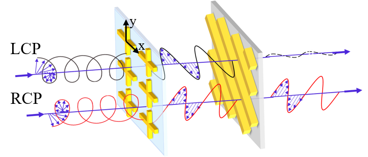
7. Ali Basiri †, Xiahui Chen, Pouya Amrollahi, Jing Bai, Joe Carpenter, Zachary Holman, Chao Wang *, and Yu Yao *, “Nature-Inspired Chiral Metasurfaces for On-Chip Circularly Polarized Light Detection,” Light: Science & Applications, vol. 8, Article number: 78, 2019. (Link: https://www.nature.com/articles/s41377-019-0184-4) |
| Chiral metamaterials and metasurfaces enable ultra-compact devices for circularly polarized light generation, manipulation and detection. Here we report bioinspired chiral metasurfaces with both strong chiral optical effect and low insertion loss. We have demonstrated experimentally sub-micron-thick circularly polarized light filters with extinction ratios up to 35 and transmission efficiency close to 80% at near infrared wavelengths (from 1.3 to 1.6 µm). We have also monolithically integrated the microscale circular polarization filters with linear polarization filters to perform full Stokes polarimetric measurement of light with arbitrary polarization state. With the advantages in easy on-chip integration, ultra-compact footprint, scalability, and broad wavelength coverage, our designs hold great promise to enable chip-integrated polarimeters and polarimetric imaging systems for quantum-based optical computing and information processing, circular dichroism spectroscopy, biomedical diagnosis and remote sensing applications. |
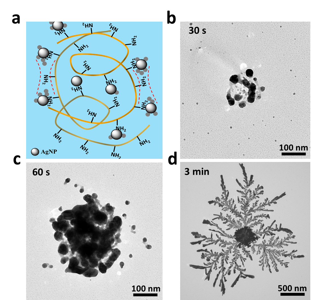 |
6. Zhi Zhao †, Ninad Chamele, Michael Kozicki, Yu Yao, and Chao Wang *, “Photochemical Synthesis of Dendritic Silver Nano-particles for Anti-counterfeiting,” J. Mater. Chem. C, vol. 7, pp. 6099-6104, 2019. (Link: https://pubs.rsc.org/en/content/articlehtml/2019/tc/c9tc01473j) |
| High-trust anti-counterfeit methodologies that produce unclonable tags on only the genuine goods are in high demand globally in a number of industries from luxury brands to smart phones and to medical and manufacturing equipment. However, prevalent tagging methods face challenges in lowering the manufacturing cost, improving the structural reliability, and simplifying readout procedures. Here we report a one-pot photochemical synthetic method to produce large quantities of dendritic silver nano-particles (AgNPs) within 20 minutes and under ambient conditions, promising for large-scale manufacturing of physical taggants. By tuning the experimental conditions, such as the UV illumination and the concentration of silver-reducing agent, poly(allylamine), we demonstrate the feasibility of creating unique dendritic AgNPs with distinctive morphological characteristics. .. |
 |
5. Benjamin H. Wunsch, Sung-Cheol Kim, Stacey M. Gifford, Yann Astier, Chao Wang, Robert L. Bruce, Jyotica V. Patel, Elizabeth A. Duch, Simon Dawes, Gustavo Stolovitzky, and Joshua T. Smith, “Gel-on-a-chip: continuous, velocity-dependent DNA separation using nanoscale lateral displacement”, Lab on a Chip, vol. 19, pp. 1567-1578, 2019. (Link: https://pubs.rsc.org/en/content/articlehtml/2019/lc/c8lc01408f) |
| We studied the trajectories of polymers being advected while diffusing in a pressure driven flow along a periodic pillar nanostructure known as nanoscale deterministic lateral displacement (nanoDLD) array. We found that polymers follow different trajectories depending on their length, flow velocity and pillar array geometry, demonstrating that nanoDLD devices can be used as a continuous polymer fractionation tool. As a model system, we used double-stranded DNA (dsDNA) with various contour lengths and demonstrated that dsDNA in the range of 100–10000 base pairs (bp) can be separated with a size-selective resolution of 200 bp… |
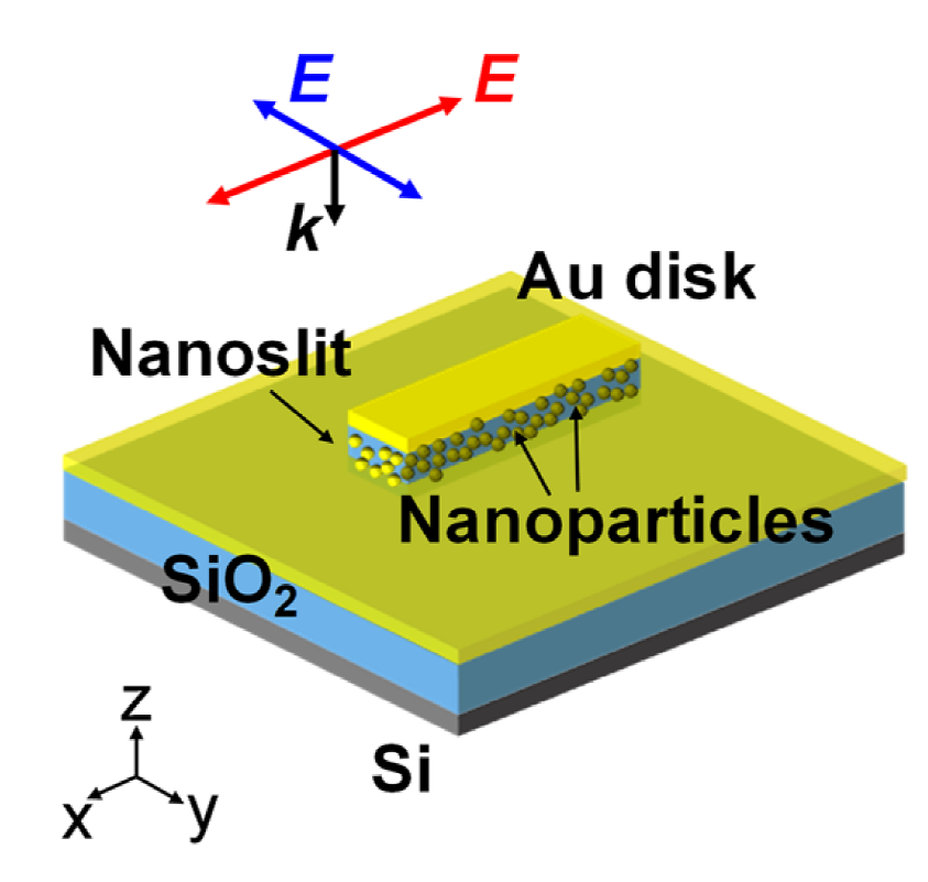 |
4. Xiahui Chen†, Chu Wang, Yu Yao *, and Chao Wang *, “Plasmonic Vertically Coupled Complementary Antennas for Dual-Mode Infrared Molecule Sensing,” ACS Nano, vol. 11, pp. 8034-8046, 2017. (Link: https://pubs.acs.org/doi/full/10.1021/acsnano.7b02687) |
| Here we report an infrared plasmonic nanosensor for label-free, sensitive, specific, and quantitative identification of nanometer-sized molecules. The device design is based on vertically coupled complementary antennas with densely patterned hot-spots. The elevated metallic nanobars and complimentary nanoslits in the substrate strongly couple at vertical nano-gaps between them, resulting in dual-mode sensing dependent on the light polarization parallel or perpendicular to the nanobars. We demonstrate experimentally that a monolayer of octadecanethiol (ODT) molecules (thickness 2.5 nm) leads to significant antenna resonance wavelength shift over 136 nm in the parallel mode, corresponding to 7.5 nm for each carbon atom in the molecular chain or 54 nm for each nanometer in analyte thickness. Additionally, all the four characteristic vibrational fingerprint signals, including the weak CH3- modes, are clearly delineated experimentally in both sensing modes. Such a dual-mode sensing with a broad wavelength design range (2.5 µm to 4.5 µm) is potentially useful for multi-analyte detection… |
 |
3. Chao Wang†*, Sung-Wook Nam †, John. M. Cotte, Christopher. V. Jahnes, Evan G. Colgan, et al., “Wafer-Scale Integration of Sacrificial Nanofluidic Chips for Single DNA Molecule Detection and Manipulation,” Nature Communications, vol. 8, pp. 14243, 2017. (Link: https://www.nature.com/articles/ncomms14243) (Download) |
| Wafer-scale fabrication of complex nanofluidic systems with integrated electronics is essential to realizing ubiquitous, compact, reliable, high-sensitivity and low-cost biomolecular sensors. Here we report a scalable fabrication strategy capable of producing nanofluidic chips with complex designs and down to single-digit nanometer dimensions over 200 mm wafer scale. Compatible with semiconductor industry standard complementary metal-oxide semiconductor (CMOS) logic circuit fabrication processes, this strategy extracts a patterned sacrificial silicon layer through hundreds of millions of nanoscale vent holes on each chip by gas-phase Xenon difluoride etching. Using single-molecule fluorescence imaging, we demonstrate these sacrificial nanofluidic chips can function to controllably and completely stretch lambda DNA in a two-dimensional nanofluidic network comprising channels and pillars… |
 |
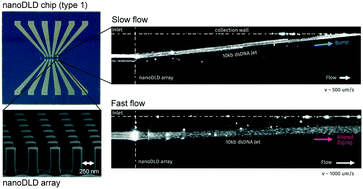
2.Benjamin H. Wunsch †, Joshua T. Smith, Stacey M. Gifford, Chao Wang, Markus Brink, Robert Bruce, Robert H. Austin, Gustavo Stolovitzky, and Yann Astier, “Nanoscale Lateral Displacement Arrays for Separation of Exosomes and Colloids Down to 20nm,” Nat. Nanotechnol., vol. 11, pp. 936–940, 2016. (Link: https://www.nature.com/articles/nnano.2016.134) |
|
To date, deterministic lateral displacement (DLD) pillar arrays have proven an efficient technology to sort, separate, and enrich micron-scale particles including human parasites, eukaryotic cells, blood cells, and circulating tumor cells in blood; however, this technology has never been translated to the true nanoscale, where it could function on bio-colloids such as exosomes. Exosomes, a key target of “liquid biopsies”, are secreted by cells, and contain information about their originating tissue, including nucleic acids and proteins. One challenge in studying exosome biology is sorting exosomes by size and surface markers. We use manufacturable silicon processes to produce nanoDLD arrays of uniform gap sizes ranging from 25 – 235 nm. Using fluorescent nanoparticles we show that at low Péclet numbers, where diffusion and deterministic displacement compete, nanoDLD arrays separate particles based on size with sharp resolution between 50 and 110 nm particles. Further, we demonstrate size-based displacement of exosomes, providing a step towards potential on-chip sorting and quantification of these important bio-colloids. This paper has been highlighted by: |
 |
1. Chao Wang †*, Robert L. Bruce, Elizabeth A. Duch, Jyotica V. Patel, Joshua T. Smith, et al., “Hydrodynamics of Diamond-Shaped Gradient Nanopillar Arrays for Effective DNA Translocation into Nanochannels,” ACS Nano, vol 9, pp. 1206-1218, 2015. (Link: https://pubs.acs.org/doi/full/10.1021/nn507350e) |
| Effective DNA translocation into nanochannels is critical for advancing genome mapping and future single-molecule DNA sequencing technologies. We present the design and hydrodynamic study of a diamond-shaped gradient pillar array connected to nanochannels for enhancing the success of DNA translocation events. Our analysis reveals the important roles of diamond-shaped nanopillars in guiding DNA into as small as 30 nm channels with minimized clogging, stretching DNA to nearly 100 % of their dyed contour length, inducing location-specific straddling of DNA at nanopillar interfaces, and modulating DNA speeds by pillar geometries. Importantly, all critical features down to 30 nm-wide nanochannels are defined using standard photolithography and fabrication processes ̶ a feat aligned with the requirement of high-volume, low-cost production. |
(2) Binquan Luan, Chao Wang, Ajay Royyuru, and Gustavo Stolovitzky, “Controlling the motion of DNA in a nanochannel with transversal alternating electric voltages,” Nanotechnology, vol 25, pp. 265101, 2014.
(3) Chao Wang, Qi Zhang, Yu Song, and Stephen Y. Chou, “Plasmonic Bar-Coupled Dots-on-Pillar Cavity Antenna with Dual Resonances for Infrared Absorption and Sensing: Performance and Nanoimprint Fabrication,” ACS Nano, vol. 8, pp. 2618-2624, 2014.
(4) Chao Wang, Sung-wook Nam, John M. Cotte, et al., “200 mm Wafer-Scale Integration of Sub-20 nm Sacrificial Nanofluidic Channels for Manipulating and Imaging Single DNA Molecules,” In proceeding of IEEE International Electron Devices Meeting (IEDM), 2013.
(5) Chao Wang and Stephen Y. Chou, “Integration of metallic nanostructures in fluidic channels for fluorescence and Raman enhancement by nanoimprint lithography and lift-off on compositional resist stack,” Microelec. Eng., Vol. 98, pp. 693-697, 2012.
(6) Chao Wang, Patrick F. Murphy, Nan Yao, Kevin McIlwrath, and Stephen Y. Chou, “Growth of Straight Silicon Nanowires on Amorphous Substrates with Uniform Diameter, Length, Orientation, and Location Using Nanopatterned Host-Mediated Catalyst,” Nano Letters, vol. 11, pp. 5247-5251, 2011.
(7) Chao Wang, Zengli Fu, Keith J. Morton, Wen-Di Li, and Stephen Y. Chou, “Printing of Sub-20 nm Wide Graphene Ribbon Arrays by Nanoimprinting Graphite Stamp and Electrostatic Force Assisted Bonding,” Nanotechnology, vol. 22, pp. 445301, 2011.
(8) Chao Wang, Qiangfei Xia, Wen-Di Li, Zengli Fu, Keith J. Morton, and Stephen Y. Chou, “Fabrication of a 60-nm-Diameter Perfectly Round Metal-Dot Array over a Large Area on a Plastic Substrate Using Nanoimprint Lithography and Self-Perfection by Liquefaction,” Small, vol. 6, pp. 1242-1247, 2010.
(9) Chao Wang and Stephen Y. Chou, “Self-aligned fabrication of 10 nm wide asymmetric trenches for Si/SiGe heterojunction tunneling field effect transistors using nanoimprint lithography, shadow evaporation, and etching,” J. Vac. Sci. Technol. B, vol. 27, pp. 2790-2794, 2009.
(10) Chao Wang, Zheyao Wang, Tian-Ling Ren, Yiping Zhu, Yi Yang, Xiaoming Wu, Haining Wang, Huajun Fang, and Litian Liu, “A micromachined piezoelectric ultrasonic transducer operating in d 33 mode using square interdigital electrodes,” IEEE Sensors Journal, vol. 7, pp. 967-976, 2007.
(11) Chao Wang, Tianling Ren, Zheyao Wang, Yiping Zhu, Ningxin Zhang, and Litian Liu, “Fabrication and characterization of in-plane polarized PZT films with interdigital electrodes,” Integrated Ferroelectrics, vol. 88, pp. 3-11, 2007.
(12) Chao Wang, Zheyao Wang, Tianling Ren, and Litian Liu, “Design and simulation of a novel operation mode of integrated ferroelectric micro-sensors,” Integrated Ferroelectrics, vol. 78, pp. 59-67, 2006.
(13) Zheyao Wang, Chao Wang, and Litian Liu, “Design and analysis of a PZT-based micromachined acoustic sensor with increased sensitivity,” IEEE transactions on ultrasonics, ferroelectrics, and frequency control, vol. 52, pp. 1840-1850, 2005.
- Seyedsina Mirjalili, Yeji Choi, Carmina Gallardo, Marisa Arias Neira, and Chao Wang, “Nanoparticle-assisted, Portable Detection of African Swine Fever Infection,” presented at the International Conference on Miniaturized Systems for Chemistry and Life Sciences | MicroTAS, Montréal, Canada, 2024. (Poster)
- Seyedsina Mirjalili, Md Ashif Ikbal, Ching-Wen Hou, Yeji Choi, Maziyar Kalateh Mohammadi, Laura A. VanBlargan, Laimonas Kelbauskas, Neal Woodbury, Vel Murugan, Brenda Hogue, Michael S. Diamond, and Chao Wang, “Nanoparticle-Supported, Rapid, Digital SARS-Cov-2 Neutralizing Assay,” presented at the International Conference on Miniaturized Systems for Chemistry and Life Sciences | MicroTAS, Montréal, Canada, 2024. (Poster)
- Yeji Choi, Seyedsina Mirjalili, MD Ashif Ikbal, Sean McClure, and Chao Wang, “Rapid, Electronic, Accessible Detection of SARS-CoV-2,” presented at the International Conference on Miniaturized Systems for Chemistry and Life Sciences | MicroTAS, Montréal, Canada, 2024. (Poster)
- Chao Wang, “Nanoparticle-Supported, Rapid, Electronic Detecting System for Accessible Infectious Disease Diagnosis,” presented at the International Conference on Electron, Ion and Photon Beam Technology and Nanofabrication, La Jolla, CA, 2024. (Invited)
- Seyedsina Mirjalili, Yeji Choi, Carmina Gallardo, Marisa Arias Neira, and Chao Wang, “Nanoparticle-assisted, Portable Detection of African Swine Fever Infection,” presented at the International Conference on Electron, Ion and Photon Beam Technology and Nanofabrication, La Jolla, CA, 2024. (Oral)
- Yeji Choi, Seyedsina Mirjalili, MD Ashif Ikbal, Sean McClure, and Chao Wang, “Rapid, Electronic, and Accessible Detection of COVID-19,” presented at the International Conference on Electron, Ion and Photon Beam Technology and Nanofabrication, La Jolla, CA, 2024. (Oral)
- Mohammad Altarafa, Maziyar Kalateh Mohammadi, MD Ashif Ikbal, and Chao Wang, “Rapid TNF-Alpha Quantification Using Gold Nanoparticles towards Cytokine Monitoring in Inflammatory Diseases,” presented at the International Conference on Electron, Ion and Photon Beam Technology and Nanofabrication, La Jolla, CA, 2024. (Oral)
- Nimarpreet Bamrah, Radhika Vattikunta, Liangxiao Chen, Deeksha Satyabola, and Chao Wang, “Nanopore Diameter Impact on DNA Methylation Detection Using Methyl Binding Domain Protein Tags,” presented at the International Conference on Electron, Ion and Photon Beam Technology and Nanofabrication, La Jolla, CA, 2024. (Poster)
- Jiawei Zuo, Scott Clemens, Abdulla Al Mamun, Dongyao Wang, Chao Wang, and Yu Yao, “3D Printing of Microstructured Metallic Thin-Films,” presented at the International Conference on Electron, Ion and Photon Beam Technology and Nanofabrication, La Jolla, CA, 2024. (Poster)
- Abdulla Al Mamun, Pengkun Xia, Ashiqur Rahman Laskar, Nimapreet K. Bamrah, and Chao Wang, “Sapphire Supported Aluminum Nitride Nanopore towards Stable and Low-Noise Biomolecule Sensing,” presented at the International Conference on Electron, Ion and Photon Beam Technology and Nanofabrication, La Jolla, CA, 2024. (Poster)
- Md Ashif Ikbal, Seyedsina Mirjalili, Maziyar Kalateh Mohammadi, Yeji Choi, Mohammad Altarfa, Jose Solano, Laura A. VanBlargan, Ching-Wen Hou, Michael S. Diamond, Vel Murugan, and Chao Wang, “Rapid Quantification of SARS-COV-2 Neutralizing Antibodies Using Electronic Nanoparticle Sensors ” in International Conference on Electron, Ion and Photon Beam Technology and Nanofabrication (EIPBN). San Francisco, California, 2023. (Oral)
- Shinhyuk Choi, Jiawei Zuo, Nabasindhu Das, Yu Yao, and Chao Wang, “Scalable Nanoimprint Manufacturing of Multi-layer Metasurfaces for Compact Polarimetric Imaging System,” in International Conference on Electron, Ion and Photon Beam Technology and Nanofabrication (EIPBN). San Francisco, California, 2023. (Oral)
- Chao Wang, “Digital biosensing for quantitative pathogen detection and immunity evaluation,” in University of Arizona College Of Medicine-Phoenix Basic Medical Sciences Seminar Series, 2023. (Invited)
- Chao Wang, “Digital Biosensing with Nanoparticles for Infectious Diseases,” in IEEE Nanotechnology Materials and Devices Conference. Nanjing/Virtual, 2022. (Invited)
- Chao Wang, “Nanotechnology for Infectious Disease Detection,” presented at the International Conference on Electron, Ion and Photon Beam Technology and Nanofabrication (EIPBN), New Orleans, Louisiana, 2022. (Invited Short Course)
- Shinhyuk Choi, Zhi Zhao, Jiawei Zuo, Hossain Mansur Resalat Faruque, Yu Yao, and Chao Wang, “Color Printing by Polymer-Assisted Photochemical Deposition of Metallic Thin Films,” presented at the International Conference on Electron, Ion and Photon Beam Technology and Nanofabrication (EIPBN), New Orleans, Louisiana, 2022. (Oral)
- Jiawei Zuo, Jing Bai, Shinhyuk Choi, Ali Barsiri, Xiahui Chen, Chao Wang, and Yu Yao, “Chip-Integrated Full-Stokes Polarimetric Imaging Sensor,” presented at the International Conference on Electron, Ion and Photon Beam Technology and Nanofabrication (EIPBN), New Orleans, Louisiana, 2022. (Invited)
- Pengkun Xia, Md Ashiqur Rahman Laskar, Xu Zhou, Deeksha Nolastname, Gde Bimananda Mahardika Wisna, Yinan Zhang, Rizal Hariadi, Hao Yan, and Chao Wang, “High-speed and High-resolution Readout of Multilevel Encoded DNA Origami by Sapphire-supported Nanopores,” presented at the International Conference on Electron, Ion and Photon Beam Technology and Nanofabrication (EIPBN), New Orleans, Louisiana, 2022. (Oral)
- Md Ashif Ikbal, Shoukai Kang, Xiahui Chen, Liangcai Gu, and Chao Wang, “Sensitive Optoelectronic Detection of Small Molecules Using Portable Metal Nanoparticle Readers,” presented at the International Conference on Electron, Ion and Photon Beam Technology and Nanofabrication (EIPBN), New Orleans, Louisiana, 2022. (Poster)
- Jiawei Zuo, Jing Bai, Shinhyuk Choi, Xiahui Chen, Chao Wang, and YuYao, “Chip-Integrated Full-Stokes Polarimetric Imaging Sensor,” presented at the Conference on Lasers and Electro-Optics (CLEO), San Jose, California, 2022. (Oral)
- Shinhyuk Choi, Zhi Zhao, Jiawei Zuo, Hossain Mansur Resalat Faruque, Yu Yao, and Chao Wang, “3D Color Printing by Additive Manufacturing of Metallic Thin Films,” presented at the Conference on Lasers and Electro-Optics (CLEO), San Jose, California, 2022. (Oral)
- Md Ashif Ikbal, Shoukai Kang, Xiahui Chen, Liangcai Gu, and Chao Wang, “Sensitive Optoelectronic Detection of Small Molecules Using Metal Nanoparticle Readers ” presented at the Conference on Lasers and Electro-Optics (CLEO), San Jose, California, 2022. (Oral)
- Shinhyuk Choi, Zhi Zhao, Jing Bai, Siying Liu, Yu Yao, and Chao Wang, “Additive Manufacturing towards Color Printing via Polymer-Assisted Photochemical Deposition of Metal Thin Films,” presented at the International Conference on Electron, Ion and Photon Beam Technology and Nanofabrication (EIPBN), Virtual, 2021. (Poster)
- Pengkun Xia, Jiawei Zuo, Pravin Paudel, Md Ashiqur Rahman Laskar, Siying Liu, and Chao Wang, “Fabrication of Sapphire-Supported Nanopore Sensors with Reproducible Micrometer Membranes,” presented at the International Conference on Electron, Ion and Photon Beam Technology and Nanofabrication (EIPBN), Virtual, 2021. (Poster)
- Chao Wang and Liangcai Gu, “Nanoparticle-Based Assay with Optoelectronic Readout for High-Sensitivity and Rapid Detection of Infectious Diseases,” presented at the International Conference on Electron, Ion, and Photon Beam Technology and Nanofabrication (EIPBN 2021), Virtual, 2021. (Invited)
- Xiahui Chen, Shoukai Kang, Zhi Zhao, Ashif Ikbal, Jiawei Zuo, Yu Yao, Liangcai Gu, and Chao Wang, “A Colorimetric Assay with Optoelectronic Readout for High-Sensitivity and Rapid Detection of Infectious Diseases “, presented at the Conference on Lasers and Electro-Optics (CLEO), Virtual, 2021. (Oral)
- Pengkun Xia, Jiawei Zuo, Shinhyuk Choi, Xiahui Chen, Jing Bai, and Chao Wang, “Sapphire-Supported Nanopores For Low-Noise DNA Sensing”, The 34th IEEE International Conference on Micro Electro Mechanical Systems (IEEE MEMS 2021) Virtual, 2021. (Oral)
- Chao Wang, “Low-noise Sapphire based Nanopore Sensors,” presented at the IEEE Nanotechnology Materials and Devices Conference, Virtual, 2020. (Invited)
- Yu Yao, Jing Ba, Ali Basiri, Xiahui Chen, Jiawei Zuo, and Chao Wang, “Highly efficient on-chip integratable metamaterials for polarimetric detection and imaging,” presented at the 2020 Lawrence symposium on epitaxy, Scottsdale, AZ, 2020. (Oral)
- Zhi Zhao, Jing Bai, Yu Yao, and Chao Wang, “Printing continuous metal structures via polymer-assisted photochemical deposition,” presented at the 2020 Lawrence symposium on epitaxy, Scottsdale, AZ, 2020. (Oral)
- Zhi Zhao, Ninad Chamele, Michael Kozicki, Yu Yao, and Chao Wang, “Photochemical Synthesis of Dendritic Silver Nano-particles (AgNPs) for Anti-counterfeiting,” presented at the The International Conference on Electron, Ion, and Photon Beam Technology and Nanofabrication Minneapolis, MN, 2019. (Oral)
- Zhi Zhao, Chao Wang, Yan Liu, and Hao Yan, “Soft Robotics Programmed with Double Crosslinking DNA Hydrogels,” presented at the The International Conference on Electron, Ion, and Photon Beam Technology and Nanofabrication Minneapolis, MN, 2019. (Oral)
- Zhi Zhao, Xiahui Chen, Ali Basiri, Yu Yao, Yan Liu, Hao Yan, and Chao Wang, “DNA Origami-Templated Assembly of Heterogeneous Nanocavity for Quantum Emitter,” presented at the The International Conference on Electron, Ion, and Photon Beam Technology and Nanofabrication Minneapolis, MN, 2019. (Oral)
- Ali Basiri, Xiahui Chen, Jing Bai, Pouya Amrollahi, Joe Carpenter, Zachary Holman, Chao Wang, and Yu Yao, “Nature-Inspired Chiral Metasurfaces for Circular Polarization Detection and Full-Stokes Polarimetric Measurement,” presented at the The International Conference on Electron, Ion, and Photon Beam Technology and Nanofabrication Minneapolis, MN, 2019. (Oral)
- Pengkun Xia, Jiawei Zuo, Pravin Paudel, and Chao Wang, “Scalable fabrication of triangular nanopore membranes on sapphire substrate for low-noise DNA detection,” presented at the The International Conference on Electron, Ion, and Photon Beam Technology and Nanofabrication Minneapolis, MN, 2019. (Oral)
- Chao Wang, “Probing Light-Matter Interaction at Quantum Scale Enabled by DNA Origami,” presented at the Biodesign Center for Molecular Design and Biomimetics Symposium, Tempe, AZ, 2018. (Oral)
- Jing Bai, Chu Wang, Xiahui Chen, Ali Basiri, Chao Wang, and Yu Yao, “Chip Integrated Plasmonic Flat Optics for Mid-infrared Polarization Detection,” presented at the Conference on Lasers and Electro-Optics (CLEO), San Jose, CA, 2018. (Oral)
- Ali Basiri, Xiahui Chen, Pouya Amrollahi, Jing Bai, Chao Wang, and Yu Yao, “Highly Efficient Circularly Polarized Light Detection Based on Chip-Integrated Metasurface,” presented at the Conference on Lasers and Electro-Optics (CLEO), San Jose, CA, 2018. (Oral)
- Jing Bai, Chu Wang, Xiahui Chen, Ali Basiri, Chao Wang, and Yu Yao, “Chip Integrated Plasmonic Flat Optics for Mid-infrared Polarization Detection,” presented at the Materials Research Society (MRS) meetings, Phoenix, AZ, 2018. (Oral)
- Ali Basiri, Xiahui Chen, Pouya Amrollahi, Jing Bai, Joe V. Carpenter, Zachary Holman, Chao Wang, and Yu Yao, “Highly Efficient Circularly Polarized Light Detection Based on Chip-Integrated Metasurface,” presented at the Materials Research Society (MRS) Meeting, Phoenix, 2018. (Oral)
- Xiahui Chen, Yu Yao, and Chao Wang, “A Novel Fano Resonance Based Plasmofluidic Nanoantenna for Ultrasensitive Biological Nanoparticle Detection,” presented at the Materials Research Society (MRS) meetings, Phoenix, AZ, 2018. (Poster)
- Xiahui Chen, Chu Wang, Yu Yao, and Chao Wang, “Plasmonic Vertically Coupled Complementary Antennas for Dual-Mode Infrared Molecule Sensing,” presented at the Material Research Society (MRS) Meeting, Phoenix, AZ, 2017. (Oral)
- Chao Wang, “Plasmonic nanoantennas for molecular sensing,” presented at the ASU Center for Photonic Innovations Annual Review, Tempe, AZ, 2015. (Poster)
- Chao Wang, “Nanopattering and Functional Nanostructures,” presented at the Workshop: Flexible Reconfigurable Electronics – 2D Device and Materials, Tempe, AZ, 2015. (Poster)
- Chao Wang, Chu Wang, and Yu Yao, “Multiplexed High-Security Signaling System Using Bioinspired Metasurface Nanostructures,” presented at Defense Innovation – SBIR/STTR Summit, 2015. (Poster)
- Chao Wang, Robert L. Bruce, Elizabeth A. Duch, Jyotica V. Patel, Joshua T. Smith, Yann Astier, Evan G. Colgan, Qinghuang Lin, and Gustavo Stolovitzk, “Clog-free Translocation of Long DNA in Nanofluidic Pillar Arrays and 30 nm Wide Channels: a Fabrication and Hydrodynamic Study,” presented at 18th International Conference on Miniaturized Systems for Chemistry and Life Sciences (μTAS 2014), San Antonio, TX, 2014.
- Binquan Luan, Chao Wang, Ajay Royyuru, and Gustavo A. Stolovitzky, “Controlling Motion of DNA in a Nanochannel with Transversal Alternating Voltages,” in Biophysical Society 58th Annual Meeting San Francisco, California, 2014.
- Chao Wang, Sung-wook Nam, John M. Cotte, et al., “200 mm Wafer-Scale Integration of Sub-20 nm Sacrificial Nanofluidic Channels for Manipulating and Imaging Single DNA Molecules,” in IEEE International Electron Devices Meeting (IEDM). Washington, DC, 2013.
- Chao Wang, “Nanofluidic Channels — A Promising Platform for DNA Sequencing,” in IBM Materials Research Community (MRC) Seminar Series, 2013.
- Ruoming Peng, Chao Wang, Liangcheng Zhou, et al., “Fabrication and Demonstration of Ultra-sensitive and Fast Immunoassay Platform With 3D Nanoplasmonic Cavity Antenna and Microfluidics Using Nanoimprint,” in EIPBN’13. Nashville, TN, 2013.
- Ruoming Peng, Chao Wang, Liangcheng Zhou, Qi Zhang, Weihua Zhang, and Stephen Y. Chou, “Fabrication and Demonstration of Ultra-sensitive and Fast Fluorescence Immunoassay Using Novel Nanoplasmonic Sensor inside Microfluidic Channels,” in Micro TAS 2012. Okinawa, Japan, 2012.
- Ruoming Peng, Chao Wang, Liangcheng Zhou, Qi Zhang, Weihua Zhang, and Stephen Y. Chou, “Fabrication and Performance of Ultra-sensitive, Fast, Nanoplasmonic Microfluidic Immunoassay by Large-Area High-Precision Nanoimprint,” in NNT 2012. Napa Valley, USA, 2012.
- Chao Wang, Ruoming Peng, Wen-Di Li, and Stephen Y. Chou, “Plasmonic Nano-cavity Antenna Arrays Integrated in Fluidic Systems for >20X Enhancement of Single DNA Molecule Detection”, MNE, Berlin, Germany, 2011.
- Chao Wang, Weihua Zhang, and Stephen Y. Chou, “Fabrication and Performance of Plasmonic Nano-cavity Antenna Arrays Self-aligned in Fluidic Channels for Enhancement of Single DNA Molecule Detection”, Micro TAS, Seattle, Washington, 2011.
- Ruoming Peng, Chao Wang, Wendi Li, Fei Ding, Weihua Zhang, Liangchen Zhou, and Stephen Y. Chou, “Over 20 Fold Fluorescence Enhancement of YOYO-1 Labeled DNA Using New 3D Cavity Nanoscale Plasmonic Antenna Array”, Micro TAS, Seattle, Washington, 2011.
- Chao Wang and Stephen Y. Chou, “Large-area Patterning of Au Nano-particles Self-aligned to Fluidic Channels for Enhancement of Molecule Detection”, EIPBN’11, Las Vegas, Nevada, 2011.
- Chao Wang, Qi Zhang, and Stephen Y. Chou, “Fabrication of Large-area Plasmonic Nano-cavity Antenna Array for High Efficiency Mid-and-Far Infrared Sensing”, EIPBN’11, Las Vegas, Nevada, 2011.
- Hao Chen, Chao Wang, and Stephen Y. Chou, “Extraction Efficiency Improvement of GaN-based Light-emitting Diodes Using Sub-wavelength Nanoimprinted Patterns on Sapphire Substrates”, EIPBN’11, Las Vegas, Nevada, 2011.
- Siran Li, Chao Wang, Yan Chen, and et al., “Nanofluidic Single DNA Sorter and Analyzer Fabricated by Nanoimprint and Wafer Bonding”, EIPBN’11, Las Vegas, Nevada, 2011.
- Wen-Di Li, Fei Ding, Yixing Liang, Chao Wang, and et al., “Design and Fabrication of High Enhancement Yet Wafer-Scale Uniform SERS/Plasmonic Structures Based on Nanoimprint Lithography and Self-Assembly”, EIPBN’11, Las Vegas, Nevada, 2011.
- Hao Chen, Chao Wang, and Stephen Y. Chou, “Extraction Efficiency Improvement of GaN Light-emitting Diode Using Sub-wavelength Nanoimprinted Patterns on Sapphire Substrate”, CLEO’11, Baltimore, Maryland, 2011.
- Chao Wang, Hao Chen, and Stephen Y. Chou, “Light Extraction Efficiency Improvement of Blue GaN Light Emitting Diode Using Nanoimprinted Patterns on Sapphire Substrate,” NNT’09, Oresund and Copenhagen, 2010.
- Chao Wang, Patrick F. Murphy, Nan Yao, and et al., “Growth of Straight Crystal Silicon Nanowires on Nanopatterned Amorphous Substrate with Uniform Diameter and Length, Preferred Orientation, and Predetermined Location,” EIPBN’10, Anchorage, Alaska, 2010.
- Wen-Di Li, Chao Wang, and Stephen Y. Chou, “100 nm Metallic Checkerboard by Wafer-scale Nanoimprint and Its Application in Surface Enhanced Raman Scattering”, CLEO’10, San Jose, California, 2010.
- Chao Wang, Qiangfei Xia, Wen-Di Li, et al., “Fabrication of Uniform Dense Metal Dot Arrays over a Large Area on Flexible Plastic Substrate Using UV Nanoimprint Lithography and Self-Perfection by Liquefaction (SPEL),” NNT’09, San Jose, California, 2009.
- Wen-Di Li, Chao Wang, and Stephen Y. Chou, “Fabrication of Large-Area 100 nm Checker Board Mold Using 3D Patterning with Multiple Nanoimprint Lithography and Self-Aligned Selective Etching”, EIPBN’09, Marco Island, Florida, 2009.
- Chao Wang, Zengli Fu, Wen-Di Li, and Stephen Y. Chou, “Printing of Sub- 20 nm Wide Graphene Ribbon Arrays over a Large Area by Imprinting Nanostructures on a Graphite Stamp and Electrostatic Force Assisted Bonding,” NNT’09, San Jose, California, 2009.
- Chao Wang and Stephen Y. Chou, “Self-Aligned Fabrication of 10 nm-Wide Asymmetric Trenches in Si for Heterojunction Tunneling FETs Using Nanoimprint Lithography, Shadow Evaporation, and Etching,” EIPBN’09, Marco Island, Florida, 2009.
- Tianling Ren, Hao Chen, Yi Yang, Yiping Zhu, Di Fu, Chao Wang, Xiaoming Wu, Jian Cai, Litian Liu, and Zhijian Li, “Micromachined piezoelectric acoustic device,” in International Workshop on Electron Devices and Semiconductor Technology (IEDST), 2009, pp. 1-6.
- Chao Wang, Patrick F. Murphy, and Stephen Y. Chou, “Location-, Diameter-, Length-, and Orientation- Controlled Growth of Si Nanowires on Amorphous Substrate Using Nanoimprint Lithography and Novel Catalysts,” NNT’08, Kyoto, Japan, 2008.
- Yiping Zhu, Tianling Ren, Chao Wang, Zheyao Wang, Litian Liu, and Zhijian Li, “Novel In-Plane Polarized PZT Film Based Ultrasonic Micro-Acoustic Device,” in International Solid-State Sensors, Actuators and Microsystems Conference (TRANSDUCERS), 2007, pp. 1291-1294.
Issued patents (26):
- Deqiang Wang, Chao Wang, Binquan Luan, Ali Afzali-Ardakani, and Gustavo A, Stolovitzky, “Self-formed nanometer channel at wafer scale,” US 8945404 B2, US 8652337 B1, CN103922275A, CN103922275B, 2014.
- Jingwei Bai, Joshua T Smith, Satyavolu S Papa Rao, Chao Wang, Yann Astier, and Michael F Lofaro, “Nanogap in-between noble metals,” US 20140302675, 2014.
- Chao Wang and Ajay K Royyuru, “Field-effect Based Nanosensor for Bio-polymer Manipulation and Detection.” US 8906215 B2, US 8999130 B2, CN 104737007, DE 112013005187, WO 2014084931, 2014.
- Chao Wang, Ruoming Peng, and Stephen Y. Chou, “Microfluidic Sensors with Enhanced Optical Signals”, US 20150253321-A1, WO2014055559 A1, CN104823049A, EP2904389A1, 2015.
- Deqiang Wang, Chao Wang, George F Walker, and Gustavo A Stolovitzky, “Reduction of Entropic Barrier of Polyelectrolyte Molecules in a Nanopore Device with Agarose Gel” US Patent 20150284791 A1, 2015.
- Binquan Luan, Deqiang Wang, Chao Wang, Ajay K Royyuru, and Gustavo A. Stolovitzky, “Polynucleotide configuration for reliable electrical and optical sensing,” US 20150037787, US 20150037843, CN104342436A, 2015.
- Deqiang Wang, Chao Wang, Binquan Luan, and Gustavo A Stolovitzky, “Increasing the Capture Zone by Nanostructure Patterns,” US Patent 20150323490, 2015.
- Chao Wang, Deqiang Wang, Qinghuang Lin, and Gustavo A Stolovitzky, “Nanofluidic channels with gradual depth change for reducing entropic barrier of biopolymers,” US Patent US 9346052, US9364832, US 20150021187, US 20150024115, US 20160199833, 2015.
- Chao Wang, Deqiang Wang, Jingwei Bai, Qinghuang Lin, and Gustavo A Stolovitzky, “Nanochannel device with three dimensional gradient by single step etching for molecular detection,” US 20150252414, US 20160220996, 2015.
- Chao Wang, Joshua T. Smith, Benjamin H. Wunsch, Yann Astier, amd Gustavo A. Stolovitzky “Biopolymer Separation Using Nanostructured Arrays,” US Patent 20160146778, 2016.
- Joshua T Smith, Benjamin H Wunsch, Chao Wang, Robert L Bruce, and Yann A Astier, “Pillar Array Structure With Uniform And High-Aspect Ratio, Nanometer Gaps,” US Patent 20160144361, 2016.
- Yann A Astier, Joshua T Smith, Chao Wang, Benjamin H Wunsch, and Gustavo A Stolovitzky, “Continuous Flow, Size-Based Separation of Entities Down to The Nanometer Scale Using Nanopillar Arrays,” US Patent 20160144406, 2016.
- Yann Astier, Stephen W Bedell, Ning Li, Devendra K Sadana, William T Spratt, and Chao Wang, “On-chip molecule fluorescence detection,” US Patent 9513220, 2016.
- Chao Wang, and Gustavo A. Stolovitzky, “Nanopillar Arrays with Interfaces for Controlled Polymer Stretching and Effective Translocation into Nanochannels” US 9733232 B1, 2017.
- Joshua T. Smith, Cornelia K. Tsang, Chao Wang, and Benjamin H. Wunsch, “Direct Bond Transfer Layers For Manufacturable Sealing of Microfluidic Chips,” US 20170144149 A1, 2017.
- Chao Wang, “Low-Noise Biomolecular Sensors,” WO2018136497, US 20210132033, 2018.
- Zhi Zhao and Chao Wang, “Photochemical Method to Grow Silver Dendrites,” US 20200130066 A1, 2020.
- Zhi Zhao, Chao Wang, and Yu Yao, “Direct metal printing with stereolithography,” US 20210323065, US 11826946 B2, 2021.
- Zhi Zhao, Chao Wang, and Yu Yao, ” Additive Manufacturing of Metal Films,” US 20220275972 A1, 2022.
- Jing Bai, Chao Wang, Yu Yao, Julius Yellowhair, and Jiawei Zuo, “Autonomous Solar Field and Receiver Inspections Based on Polarimetric-Enhanced Imaging,” US 20210226583 A1, 2021.
- Yu Yao, Chao Wang, Chu Wang, Jing Bai, Ali Basiri, and Xiahui Chen, “On-Chip Polarization Detection and Polarimetric Imaging,” U.S. 20220268633, U.S. 12117344, 2022.
- Xiahui Chen, Shoukai Kang, MD Ashif Ikbal, Zhi Zhang, Liangcai Gu, and Chao Wang, “Methods, Devices, and Related Aspects for Detecting Ebola Virus,” US 20220099675, 2022.
- Chao Wang and MD Ashif Ikbal, “Compositions And Methods For Rapid Covid-19 Detection,” US 20220163522 A1, 2022.
- Chao Wang and Pengkun Xia, “Low-capacitance nanopore sensor on insulating substrates,” US 20230091639, US 11891689 B2, 2023.
- Chao Wang and Shinhyuk Choi, “Color image printing by polymer-assisted photochemical deposition,” US 20230219284 A1, 2023.
- Chao Wang and MD Ashif Ikbal, “Methods, Devices, and Related Aspects for Detecting Cannabinoids,” US 20240377418 A1, WO 2020/210743, 2024.
Pending applications (6)
- Chao Wang, Liangcai Gu, Xiahui Chen, Shoukai Kang, MD Ashif Ikbal, and Zhi Zhao, “Methods, Devices, And Related Aspects For Detecting Severe Acute Respiratory Syndrome Coronavirus-2,” Patent Application 63250023, WO/2023/056260.
- Chao Wang, Seyedsina Mirjalili, Carmina Gallardo, and Marisa Arias Neira, “Rapid and Sensitive African Swine Fever Detection,” Patent Application 63532501, disclosed 2023.
- Chao Wang, Yu Yao, Shinhyuk Choi, and Jiawei Zuo, “Scalable Design and Manufacturing of Functional Metasurfaces and Metamaterials,” Patent Application 63500458, disclosed 2023.
- Yeji Choi, Seyedsina Mirjalili, and Chao Wang, “Methods and Related Aspects for Rapid, Electronic Antigen Detection of Infectious Diseases,” Patent Application 63653410, disclosed 2024.
- Maziyar KalatehMohammadi and Chao Wang, “Methods and Related Aspects for Rapid Cytokine Detection for Inflammatory Disease Diagnosis,” Patent Application 63653383, disclosed 2024.
- MD Ashif Ikbal, Seyedsina Mirjalili, and Chao Wang, “Methods and Related Aspects for Digital Neutralizing Antibody Assays for Disease Detection and Immunity Assessment,” Patent Application 63653356, disclosed 2024.