Nanophotonics and metasurface
Metallic and dielectric nanostructures have been widely used to spatially, temporally, or spectrally modulate the refractive indexes of materials-of-interest and to engineer the amplitude, phase and polarization response. My lab leverages our expertise in nanomanufacturing to explore new nano-scale photonic phenomena. In collaboration with Dr. Yu Yao, we are developing metasurface structures, devices and systems for polarization imaging and detection. In addition, we explore plasmonic structures for molecular sensing.
Metasurface nanostructures for polarization control and sensing
Circularly polarized light (CPL) has been widely utilized in quantum communication, quantum computing, circular dichroism (CD) spectroscopy and polarimetric imaging and sensing. Traditionally, CP light detection requires multiple bulky optical elements such as polarizers, waveplates and mechanically rotating components, which pose fundamental limitations for device miniaturization, robust system integration and high-speed operation. Recent developments in nanotechnology and nanophotonics have enabled ultra-compact solid-state CPL detection that generally exhibit superior stability in ambient conditions, fast response time and high fidelity. For example, artificial three-dimensional (3D) metamaterials have been demonstrated based on chiral nanostructures to differentiate opposite handedness of CPL. However, fabrication of such complex 3D structures requires stringent process control and its scalability is challenging. More recently, planar (or 2D) chiral plasmonic metasurface structures have also been reported with chiro-optical responses. Compared with 3D chiral metamaterials, the metasurface structures are easier to fabricate and more compatible with on-chip manufacturing technologies; yet, the chiral plasmonic metasurfaces experimentally demonstrated so far usually suffer from low Circular Polarization Extinction Ratios (CPERs) (less than ~5) and limited optical efficiency in experiment (20-50 %). To improve the optical efficiency, chiral dielectric metasurface structures have been achieved in experiment, with optical efficiency up to 90 %. However, their CPERs are still limited (up to 8). To date, it is still challenging to realize ultra-compact CPL detection devices with simultaneously high extinction ratio and optical efficiency.
Inspired by the compound eyes of Stomatopods, we have recently demonstrated theoretically and experimentally double-layer chiral metasurface structures for near-infrared wavelength polarimetric detection with a CPER up to 35 and transmission efficiency >80%. The structure consists of a low-loss dielectric metasurface, an oxide spacer layer and a nanowire polarizer, with a total thickness of less than 1 µm. Besides CPL detection units, we have also integrated the chiral metasurface structures on the same chip with linear polarization (LP) filters to perform full-stokes polarimetric detection. Our designs are advantageous for its feasibility of direct and scalable integration onto existing imaging sensors, high extinction ratio, high transmission efficiency, ultra-compact footprint (sub-wavelength thickness, micrometer scale in lateral dimension) and robustness; thus are ideal for ultra-compact imaging, sensing, communication and navigation systems.
Reference:
- Ali Basiri, Xiahui Chen, Pouya Amrollahi, Jing Bai, Joe Carpenter, Zachary Holman, Chao Wang *, and Yu Yao *, “Nature-Inspired Chiral Metasurfaces for On-Chip Circularly Polarized Light Detection,” Light: Science & Applications, 8, pp. 78, 2019. https://doi.org/10.1038/s41377-019-0184-4
- Jing Bai, Chu Wang, Xiahui Chen, Ali Basiri, Chao Wang, and Yu Yao *, “On Chip-Integrated Plasmonic Flat Optics for Mid-Infrared Full-Stokes Polarization Detection,” Photonics Research, vol. 7, pp. 1051-1060, 2019.
Device integration and large-scale nanoimprint manufacturing
A desirable polarization imaging system should be compact, fast, and capable of perform accurate polarization measurement over a broad wavelength range and large angle of view, which, however, remain elusive. Very recently we successfully demonstrated a chip-integrated Metasurface-based Full-Stokes Polarimetric Imaging sensor (MetaPolarIm) by integrating an ultrathin (~600 nm) metasurface polarization filter array (MPFA) onto a visible imaging sensor with CMOS compatible fabrication processes. The MPFA is featured with broadband dielectric-metal hybrid chiral metasurfaces and double-layer nanograting polarizers. This chip-integrated polarimetric imaging sensor enables single-shot full-Stokes imaging (speed limited by the CMOS imager) with the most compact form factor, record high measurement accuracy, dual-color operation (green and red) and a field of view up to 40 degrees. MetaPolarIm holds great promise to enable transformative applications in autonomous vision, industry inspection, space exploration, medical imaging and diagnosis.
On the other hand, scalable nanomanufacturing of metasurfaces with high uniformity and reproducibility is key to technology transfer and commercialization. Recently, nanoimprint lithography (NIL) has attracted increasing interests for metasurface fabrication because of its superior nanometer resolution, rapid prototyping and large-area manufacturing capabilities. Despite NIL demonstrations of single-layer metasurface, scalable fabrication of double- and multi-layer metasurfaces remains challenging. Here we leverage the high resolution and 3D pattern transfer capabilities of NIL to collaboratively design and fabricate multi-layered metasurfaces for on-chip polarimetric imaging devices. Our process achieved sub-100 nm nanostructures, sub-200 nm alignment accuracy, and nanometer-scale linewidth uniformity over >20 mm2. This NIL-based, low-cost and high-throughput nanomanufacturing approach paves the way toward scalable production of a plethora of metasurface structures for ultra-compact optic and optoelectronic devices and systems.
Reference:
- Jiawei Zuo, Jing Bai, Shinhyuk Choi, Ali Basiri, Xiahui Chen, Chao Wang, and Yu Yao*, “Chip-Integrated Full-Stokes Polarimetric CMOS Imaging Sensor,” Light: Science & Applications, vol. 12, pp. 218, 2023. https://doi.org/10.1038/s41377-023-01260-w.
- Shinhyuk Choi†, Jiawei Zuo†, Nabasindhu Das, Yu Yao*, and Chao Wang*, ” Scalable Nanoimprint Manufacturing of Functional Multilayer Metasurface Devices,” Advanced Functional Materials, 2404852, 2024. https://doi.org/10.1002/adfm.202404852
- Jiawei Zuo, Ashutosh Bangalore Aravinda Babu, Mo Tian, Jing Bai, Shinhyuk Choi, Hossain Mansur Resalat Faruque, Smitha S. Swain, Michael N. Kozicki, Chao Wang, and Yu Yao*, “Metasurface-Based Muller Matrix Microscope,” Advanced Functional Materials, 2405412, DOI: 10.1002/adfm.202405412, 2024. https://doi.org/10.1002/adfm.202405412

Plasmonic Biosensing
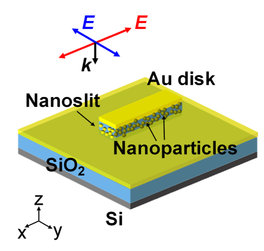
Recently, we reported a plasmonic nanosensor for label-free, sensitive, specific, and quantitative identification of nanometer-sized molecules in the infrared range. The device design is based on vertically coupled complementary antennas with densely patterned hot-spots. The elevated metallic nanobars and complimentary nanoslits in the substrate strongly couple at vertical nano-gaps between them, resulting in dual-mode sensing dependent on the light polarization parallel or perpendicular to the nanobars. We demonstrate experimentally that a monolayer of octadecanethiol (ODT) molecules (thickness 2.5 nm) leads to significant antenna resonance wavelength shift over 136 nm, corresponding to 7.5 nm for each carbon atom in the molecular chain or 54 nm for each nanometer in analyte thickness. Additionally, all the four characteristic vibrational fingerprint signals, including the weak CH3– modes, are clearly delineated experimentally in both sensing modes. Such a dual-mode sensing with a broad wavelength design range (2.5 µm to 4.5 µm) is potentially useful for multi-analyte detection.
Reference:
- Xiahui Chen, Chu Wang, Yu Yao *, and Chao Wang *, “Plasmonic Vertically Coupled Complementary Antennas for Dual-Mode Infrared Molecule Sensing,” ACS Nano, 11, pp. 8034-8046, 2017.